|
The electro-phototic modulator accomplishes the conversion function from electrical signal to optical signal and is one of the key components of optical interconnect, optical computing and optical communication systems. Silicon-based photonic devices have been the most attractive research hotspot in the field of optoelectronics in the past decade. The silicon-based electro-optic modulators have become the iconic devices representing the development level of silicon-based photonics due to their complex structure and important electro-optical conversion functions. The research team carried out systematic and in-depth research on silicon-based electro-optic modulators, and firstly realized silicon-based electro-optic modulators with modulation rates of up to 60 Gb/s, and carried out related research on packaging and other fields, ranking the world's leading level.
|
|
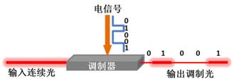
Figure 1 Schematic diagram of electro-optic modulator
|
|
In silicon-based electro-optic modulators, the most widely used modulation mechanism is the plasma dispersion effect: an applied electric field changes the carrier concentration in the silicon waveguide, thereby changing the waveguide refractive index and absorption coefficient. The silicon-based modulator based on the plasma dispersion effect consists of two parts——an optical structure and an electrical structure: the optical structure guides the direction of light propagation in the waveguide, and converts the phase modulation introduced by the electrical structure into light intensity modulation; the electrical structure changes The carrier distribution in the silicon-based optical waveguide changes the refractive index of the waveguide, thereby changing the phase of the transmitted light in the waveguide, and converting the phase change into a change in light intensity through the interference structure or the resonant cavity structure.
The optical structures commonly used in modulators are Mach-Zehnder interferometer (MZI) type and micro-ring resonator (MRR) type, as shown in Fig. 2. In the MZI type modulator, the incident light is coupled into the beam splitter of the modulator, and is split into two beams respectively into the MZI two-arm waveguide, and then combined by the combiner, and the interference superposition constitutes the output light. If the carrier distribution in the modulated arm waveguide changes due to the plasma dispersion effect, the phase of the transmitted light will change, and the power modulation function of the light is realized by interference. In the MRR type modulator, the incident light enters the straight waveguide and is partially coupled into the micro-wave. The light field of the ring, the straight waveguide and the light field coupled from the micro-ring into the straight waveguide are superimposed to form the light field of the output light. Changing the refractive index of the micro-ring waveguide by the electrical structure will change the phase of the transmitted light in the micro-ring, thereby changing the interference superposition effect and realizing the modulation function.
|
|
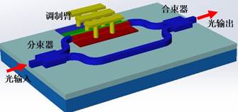 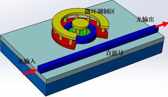
Figure2. Schematic diagram of MZI type and MRR type modulator
|
|
The silicon-based modulators based on the plasma dispersion effect commonly have electrical structures such as MOS capacitor type, forward PIN type, and reverse PN type, etc. The MOS capacitor type structure is formed by inserting a gate oxide layer in the ridge waveguide to form a capacitor structure. When a bias voltage is applied, carrier accumulation is formed on both sides of the gate oxide layer, and the refractive index of the ridge waveguide is changed;the PIN type structure is formed by the ridge waveguide in the intrinsic rigion and the heavily doped plate region on both sides of the P region and the N region. When a forward bias is applied, a large amount of unbalanced minority carriers are injected into the intrinsic region to change the refractive index of the ridge waveguide. In the rib waveguide of the reverse PN type structure, the lightly doped P and N regions are applied. When reverse bias is applied, the width of the depletion region is increased, the existing carriers in the waveguide are reduced, and the refraction rate of the ridge waveguide is changed.
|
|
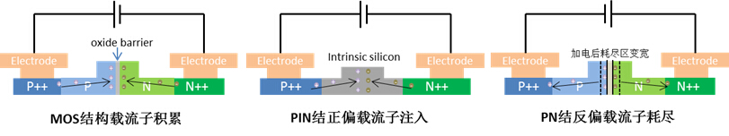
Figure 3. Schematic diagram of common electrical structure
|
|
Silicon-based electro-optic modulators have been one of the most popular research hotspots in the field of optoelectronics in the past decade. In 2004, Intel first realized silicon-based modulators above 1Gb/s. In recent years, the University of Surrey in the United Kingdom, the University of Paris-Sud in France, the PETRA in Japan, the Alcatel-Lucent in the United States, the Oracle in Singapore, and the IME in Singapore have all implemented 40-50 Gb/s silicon-based modulators. The research on silicon-based modulators in China has been carried out earlier, but the research is in a tracking state for a long time.
After 2012, under the support of the national major scientific research plan “Study on Silicon-based Micro-nano Waveguide Structure Light Modulators and Optical Switching Arrays and Integrated Chips”, the research of silicon-based modulators has made a major breakthrough. From the end of 2012 to the beginning of 2013, the modulation rates of silicon-based modulators such as MZI and MRR were up to 60Gb/s, ranking first in the world at the time. The results were invited to the European Optical Communication Conference ECOC2013, one of the top conferences of international optical communication. It was published as the only invitation report in China. In 2014, the research team took full advantage of the design advantages and broke through the limitations of multiple processes and structural parameters that could not be freely set in the multi-project wafer sharing (MPW) manufacturing model. The standard 220nm top silicon structure was used and developed by IME-MPW. A successful high-speed silicon-based modulator with a modulation rate of 64 Gb/s, reaching the limits of existing test systems. At the same time, the research group carried out research on high-frequency module packaging of modulators. In November 2014, the company first developed the first silicon-based electro-optic modulator package module with a modulation rate of 20Gb/s, which is practical for silicon-based modulators. Foundation.
|
|